01
Monolithic 2T architecture
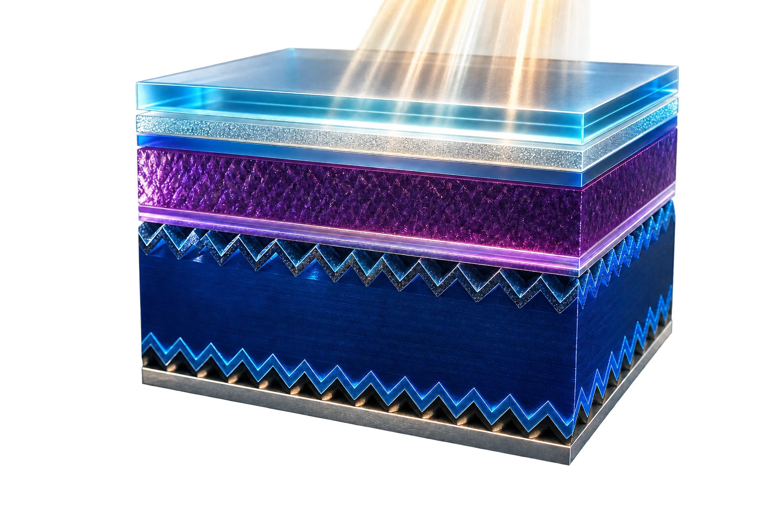
Top and bottom cells are monolithically series-connected with only two external terminals—a more compact structure with a clearer encapsulation path.

2T PEROVSKITE–SILICON TANDEM
Monolithic integration. Two junctions in sync. Built for next-generation, high-power-density photovoltaics.
MONOLITHIC VIEWEXPLODED LAYER VIEW
01
Top and bottom cells are monolithically series-connected with only two external terminals—a more compact structure with a clearer encapsulation path.
02
High-energy photons go to wide-bandgap perovskite, while silicon continues to harvest near-infrared light. Every photon meets the absorber suited to it.
03
More output from the same illuminated area unlocks value for rooftops, mobile energy and other space-constrained applications.
COMPANY FILM
Step inside tandem R&D and manufacturing, where materials, devices and nanoscale processes come together to advance next-generation photovoltaics.
2T ARCHITECTURE
The perovskite top cell and silicon bottom cell are series-connected through a recombination junction. No external spectral splitter. No four-terminal wiring. The complexity stays inside the microstructure, leaving modules and systems elegantly simple.
NANOSCALE PROCESS
Critical functional layers can be as thin as 1 nm. Precise control of thickness and interfaces brings optics, electronics and stability into concert at the smallest scale.

01 / OPTICAL ENTRY
Anti-reflection and transparent conductive layers work together to create a low-loss entry for short-wavelength light while maintaining lateral carrier transport.
SPECTRUM MANAGEMENT
A single-junction silicon cell must handle the entire solar spectrum alone. A 2T tandem assigns each bandgap the work it does best—reducing thermalization losses from high-energy photons while preserving silicon's response to long-wavelength light.
PERFORMANCE PATH
30%+
Target values vary with area, device architecture, material system and third-party test conditions.
Subcell voltages add, while current matching determines total output.
Retains familiar module interconnection logic and reduces system integration complexity.
More output per square metre for space-limited, high-value energy applications.
RELIABILITY
Efficiency is only the beginning. Interface stability, ion migration, encapsulation barriers and thermomechanical matching together determine how far a tandem device can go.
FROM LAYER TO DEVICE
Microstructure, film uniformity and current–voltage response together provide the evidence for device diagnostics.
Tracks interlayer expansion mismatch, interface stress and electrical performance drift.
Validates encapsulation barriers, ion migration and long-term moisture and oxygen stability.
Evaluates the photochemical durability of wide-bandgap absorbers and interface materials.
Covers transportation, installation, wind and snow loads, and module deformation.
APPLICATIONS
ROOFTOP / BIPV
When area is scarcer than module cost, power per square metre becomes system value.
MOBILE ENERGY
For vehicle roofs, portable equipment and off-grid systems, with less dependence on deployable area.
HIGH ALTITUDE / SPACE
Thinner cells, lower mass and broader spectral utilization for high-altitude and space power systems.
WHY UPGRADE
NEXT-GENERATION PV
Get technical roadmaps, device architecture and application materials.
Contact us